- 您现在的位置:买卖IC网 > Sheet目录308 > ADUM1286CRZ (Analog Devices Inc)ISOLATOR DGTL 3KVRMS 2CH 8-SOIC
Data Sheet
ADuM1280/ADuM1281/ADuM1285/ADuM1286
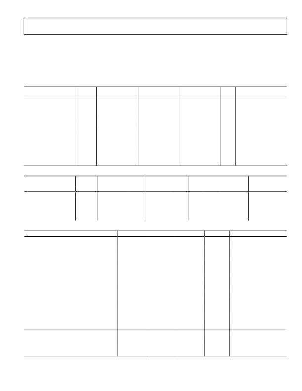
SPECIFICATIONS
ELECTRICAL CHARACTERISTICS—5 V OPERATION (ALL GRADES)
All typical specifications are at T A = 25°C, V DD1 = V DD2 = 5 V. Minimum/maximum specifications apply over the entire recommended
operation range: 4.5 V ≤ V DD1 ≤ 5.5 V, 4.5 V ≤ V DD2 ≤ 5.5 V, ?40°C ≤ T A ≤ 125°C, unless otherwise noted. Switching specifications are
tested with C L = 15 pF and CMOS signal levels, unless otherwise noted.
Table 1.
A, WA Grades
B, WB Grades
C, WC Grades
Parameter
Symbol
Min
Typ
Max
Min
Typ
Max
Min
Typ
Max
Unit
Test Conditions
SWITCHING SPECIFICATIONS
Pulse Width
Data Rate
PW
1000
1
40
25
10
100
ns
Mbps
Within PWD limit
Within PWD limit
Propagation Delay
Pulse Width Distortion
t PHL , t PLH
PWD
50
10
35
3
13
18
24
2
ns
ns
50% input to 50% output
|t PLH ? t PHL |
Change vs. Temperature
7
3
1.5
ps/°C
Propagation Delay Skew
t PSK
38
12
9
ns
Between any two units at
same operating conditions
Channel Matching
Codirectional
Opposing Direction
Jitter
t PSKCD
t PSKOD
2
5
10
2
3
6
1
2
5
ns
ns
ns
Table 2.
1 Mbps–A, B, C,WA, WB,
WC Grades
25 Mbps–B, C, WB,
WC Grades
100 Mbps–C, WC
Grades
Parameter
Symbol
Min
Typ
Max
Min
Typ
Max
Min
Typ
Max
Unit
Test Conditions
SUPPLY CURRENT
No load
ADuM1280 / ADuM1285
ADuM1281 / ADuM1286
I DD1
I DD2
I DD1
I DD2
1.1
2.7
2.1
2.3
1.6
4.5
2.6
2.9
6.2
4.8
4.9
4.7
7.0
7.0
6.0
6.4
20
9.5
15
15.6
25
15
19
19
mA
mA
mA
mA
Table 3. For All Models
Parameter
Symbol
Min
Typ
Max
Unit
Test Conditions
DC SPECIFICATIONS
Logic High Input Threshold
Logic Low Input Threshold
V IH
V IL
0.7 V DDx
0.3 V DDx
V
V
Logic High Output Voltages
V OH
V DDx ? 0.1
V DDx ? 0.4
5.0
4.8
V
V
I Ox = ?20 μA, V Ix = V IxH
I Ox = ?4 mA, V Ix = V IxH
Logic Low Output Voltages
V OL
0.0
0.2
0.1
0.4
V
V
I Ox = 20 μA, V Ix = V IxL
I Ox = 4 mA, V Ix = V IxL
Input Current per Channel
I I
?10
+0.01
+10
μA
0 V ≤ V Ix ≤ V DDx
Supply Current per Channel
Quiescent Input Supply Current
Quiescent Output Supply Current
Dynamic Input Supply Current
Dynamic Output Supply Current
I DDI(Q)
I DDO(Q)
I DDI(D)
I DDO(D)
0.54
1.6
0.09
0.04
0.8
2.0
mA
mA
mA/Mbps
mA/Mbps
Undervoltage Lockout
Positive V DDx Threshold
Negative V DDx Threshold
V DDx Hysteresis
V DDXUV+
V DDXUV-
V DDXUVH
2.6
2.4
0.2
V
V
V
AC SPECIFICATIONS
Output Rise/Fall Time
t R /t F
2.5
ns
10% to 90%
Common-Mode Transient Immunity 1
|CM|
25
35
kV/μs
V Ix = V DDx , V CM = 1000 V,
transient magnitude = 800 V
Refresh Period
t r
1.6
μs
1
|CM| is the maximum common-mode voltage slew rate that can be sustained while maintaining V o > 0.8 V DDx . The common-mode voltage slew rates apply to both
rising and falling common-mode voltage edges.
Rev. B | Page 3 of 20
发布紧急采购,3分钟左右您将得到回复。
相关PDF资料
ADUM1300BRW
IC DIGITAL ISOLATOR 3CH 16-SOIC
ADUM1310BRWZ
IC ISOLATOR DGTL 3CH UNI 16-SOIC
ADUM1400WTRWZ
IC ISOLATOR DIG 4CH 125C 16SOIC
ADUM1412BRWZ-RL
IC ISOLATOR DGTL QUAD 16-SOIC
ADUM1420BRWZ-RL
IC ISOLATOR DGTL 4CH 28SOIC
ADUM1510BRWZ-RL
IC DIGITAL ISOLATOR 16-SOIC
ADUM2210TRIZ
ISOLATOR DGTL 2CH 16SOIC
ADUM2250ARIZ-RL
ISOLATOR DL I2C HOT-SWAP 16SOIC
相关代理商/技术参数
ADUM1286CRZ-RL7
功能描述:ISOLATOR DGTL 3KVRMS 2CH 8SOIC RoHS:是 类别:隔离器 >> 数字隔离器 系列:* 产品培训模块:IsoLoop® Isolator 标准包装:50 系列:IsoLoop® 输入 - 1 侧/2 侧:5/0 通道数:5 电源电压:3 V ~ 5.5 V 电压 - 隔离:2500Vrms 数据速率:110Mbps 传输延迟:12ns 输出类型:CMOS 封装/外壳:16-SOIC(0.154",3.90mm 宽) 供应商设备封装:16-SOIC N 包装:管件 工作温度:-40°C ~ 85°C 其它名称:390-1053-5
ADUM1286WARZ
制造商:AD 制造商全称:Analog Devices 功能描述:3 kV RMS Dual Channel Digital Isolators
ADUM1286WARZ-RL7
功能描述:General Purpose Digital Isolator 3000Vrms 2 Channel 1Mbps 25kV/μs CMTI 8-SOIC (0.154", 3.90mm Width) 制造商:analog devices inc. 系列:iCoupler? 包装:带卷(TR) 零件状态:有效 技术:磁耦合 类型:通用 隔离式电源:无 通道数:2 输入 - 输入侧 1/输入侧 2:1/1 通道类型:单向 电压 - 隔离:3000Vrms 共模瞬态抗扰度(最小值):25kV/μs 数据速率:1Mbps 传播延迟 tpLH / tpHL(最大值):50ns,50ns 脉宽失真(最大):10ns 上升/下降时间(典型值):2.5ns,2.5ns 电压 - 电源:3 V ~ 5.5 V 工作温度:-40°C ~ 125°C 封装/外壳:8-SOIC(0.154",3.90mm 宽) 供应商器件封装:8-SOIC 标准包装:1,000
ADUM1286WBRZ
制造商:AD 制造商全称:Analog Devices 功能描述:3 kV RMS Dual Channel Digital Isolators
ADUM1286WBRZ-RL7
功能描述:General Purpose Digital Isolator 3000Vrms 2 Channel 25Mbps 25kV/μs CMTI 8-SOIC (0.154", 3.90mm Width) 制造商:analog devices inc. 系列:iCoupler? 包装:带卷(TR) 零件状态:有效 技术:磁耦合 类型:通用 隔离式电源:无 通道数:2 输入 - 输入侧 1/输入侧 2:1/1 通道类型:单向 电压 - 隔离:3000Vrms 共模瞬态抗扰度(最小值):25kV/μs 数据速率:25Mbps 传播延迟 tpLH / tpHL(最大值):35ns,35ns 脉宽失真(最大):3ns 上升/下降时间(典型值):2.5ns,2.5ns 电压 - 电源:3 V ~ 5.5 V 工作温度:-40°C ~ 125°C 封装/外壳:8-SOIC(0.154",3.90mm 宽) 供应商器件封装:8-SOIC 标准包装:1,000
ADUM1286WCRZ
制造商:AD 制造商全称:Analog Devices 功能描述:3 kV RMS Dual Channel Digital Isolators
ADUM1286WCRZ-RL7
功能描述:General Purpose Digital Isolator 3000Vrms 2 Channel 100Mbps 25kV/μs CMTI 8-SOIC (0.154", 3.90mm Width) 制造商:analog devices inc. 系列:iCoupler? 包装:带卷(TR) 零件状态:有效 技术:磁耦合 类型:通用 隔离式电源:无 通道数:2 输入 - 输入侧 1/输入侧 2:1/1 通道类型:单向 电压 - 隔离:3000Vrms 共模瞬态抗扰度(最小值):25kV/μs 数据速率:100Mbps 传播延迟 tpLH / tpHL(最大值):24ns,24ns 脉宽失真(最大):2ns 上升/下降时间(典型值):2.5ns,2.5ns 电压 - 电源:3 V ~ 5.5 V 工作温度:-40°C ~ 125°C 封装/外壳:8-SOIC(0.154",3.90mm 宽) 供应商器件封装:8-SOIC 标准包装:1,000
ADUM128X
制造商:AD 制造商全称:Analog Devices 功能描述:Digital Isolator Product Selection and Resource Guide
